Category How does It works, How things work, How is it done, Curiosity

How do you create a microchip?

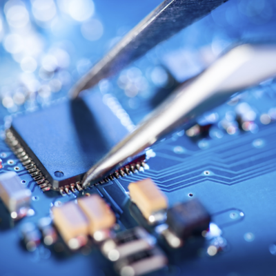
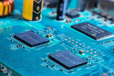
Chips are produced several hundred at a time on a slice of ultra pure, artificially formed silicon crystal, so thin that it would take about 250 slices to form a piece 1in (25mm)thick. Layout diagrams for circuits are prepared on a computer, then each reduced to chip size and set out side by side on a glass plate known as a mask. Because witches and other components are built up in separate layers on the chip, a mask is made for each operation. The masks – which block out the unwanted parts – are made many times larger than the chip and reduced photographically.

The chips are built up by forming each layer – p-type or n-type layers or insulating layers of silicon dioxide – and etching out the unwanted parts. This is done by treating the layer with a coating sensitive to ultraviolet light, masking it, then exposing it to ultraviolet light. The exposed parts become resistant to acid, but the blocked-out parts do not – they are etched away when the layer is coated with acid.

Parts such as aluminium contacts are deposited in the areas etched for them as a vapour. When hardened, the aluminium is etched to add the required circuit connections, which lead to contact pads at the edges of the chip.

All completed chips on slice are tested with delicate electrical probes to check that they are working properly. About 70 per cent prove faulty. They are marked as rejects and thrown away. After testing, the slice is cut into individual chips under a microscope with a diamond-tipped cutter. The good chips are each mounted in a frame that is encased in plastic. The contact pads are linked to metal connectors are in turn linked to protruding legs, or pins, that plug into the external circuit.


Picture Credit : Google

How a transistor works?

Transistors are the commonest components in a microchip. They are used mostly as switches, letting current through to represent the binary digit 1, or cutting it off to represent 0.

A widely used type of transistor has two islands of n-type semiconductor in a larger base of p-type. While the transistor is switched off. The free electrons from the layers drain into the p layer and are absorbed by the free holes. The transistor is switched on by applying a voltage from a separate low-power circuit to an aluminium gate above the p base. This voltage attracts the free electrons from the p base towards the gate. They then form a bridge between the two n islands and provide a path for the current through the circuit in which the switch is operating.

The transistor is switched off by cutting off the power. The free electrons then drain back to the p base and are absorbed by the free holes. Without the bridge they formed between the islands, current cannot flow through the circuit.


Picture Credit : Google

How the silicon conducts electricity?

Pure silicon is an insulator — it does not conduct electric current However, if it is impure — containing certain other elements — it will conduct a weak current. So it is called a semiconductor, halfway between an insulator and conductor. Semiconductors allow the delicate control of current needed for demonic devices, such as transistors, to an extent impossible with full conductors such as metals. A semiconductor is made by adding elements – usually phosphorus or boron — to the silicon. if a small amount of the phosphorus is introduced as a gas while the silicon crystal is being formed into a chip, the phosphorus atoms bond together with some of the silicon atoms. Four electrons in the outer layers of each type of atom pair off, but one phosphorus electron is spare, so it is left free to form an electric current when a voltage is applied. Electrons are negatively charged, so this type of crystal is called an n- type (negative) semiconductor.

If small amount of boron is mixed with the silicon, there is one electron short in the bonding system, leaving a hole that attracts five electrons. Free holes create a positive charge so the crystal is called a p-type (positive) semiconductor. These two types of semiconductor are formed in sections within one crystal for most microchip components.


Picture Credit : Google

How chips are running the world?

Within an area no bigger than a shirt button, a microchip holds as many as 450,000 electronic components. They are linked into electric circuits and are visible only under a microscope.

Microchips have transformed modern life and made some of the science fiction of the past into reality. They regulate digital watches, set programs on washing machines, and beat us at video games. They also manipulate robots on car-production lines and control national defence systems.

Electronically, the circuits that make up a microchip are not particularly complex —many are just switches. Their wizardry lies in their minute size, which allows signals to flow through at lightning speed. So they can carry out up to 250 million calculations in a second.

Most microchips are made of silicon, one of the most abundant elements on earth, and easily obtained from sand and rocks. A few are made from gallium arsenide — a compound of arsenic and the metal gallium, found in minerals such as coal.

 Chips for everything

There are various kinds of microchip. A microprocessor chip can be a computer in itself – in a washing machine, for example. Or it can be the nerve centre of a larger computer, controlling all its activities.

Memory chips store information in computers on sets of identical circuits —either permanently or temporarily. Interface chips translate the signals coming into the microprocessor from outside — such as from a keyboard — into binary code so that the electronic circuits can handle it. They also translate the outgoing signals back into figures or words for the computer screen.

Clock chips provide the timing needed for all the computer circuits to process electric signals in the right sequence. Each is linked to a quartz crystal that vibrates at a precise frequency.


Picture Credit : Google

When did the Polaroid Land camera come out?

In 1944, a child’s disappointment having to wait several days to see the photograph her father had taken led him to devise a quick method of film processing.

He was an American, Dr Edwin Land of Cambridge, Massachusetts, and in just a few months he had come up with a solution. Within three years the first instant-picture camera came on the market, capable of producing a finished black-and-white picture in about a minute. He called it the Polaroid-Land camera.

Today, a Polaroid camera can produce a black and white print in as little as ten seconds and a colour print in only a minute. The secret behind instant photography lies in the film, not in the camera. The film not only has a coating of light sensitive emulsion like a normal photographic film, but also carries the chemicals necessary to process it.

The film pack has both negative and positive sections – in a colour film each is many-layered, with dye developer layers alongside was colour-sensitive negative layer. The processing chemicals that trigger off the developing and printing process are in jelly-like form in a tiny plastic pod between the negative and positive sections.

The pod bursts when the film is removed from the camera through a pair of rollers. The chemicals are spread evenly over the film, and diffuse through it to set the picture processing in motion. The sandwich of film and print material develops in daylight outside the camera, and a positive picture is revealed when the negative and positive layers are pulled apart.


Picture Credit : Google

What are the types of camera?

Two of the mist widely used cameras are the compact and the single-lens reflex (SLR). Both use 35mm film, although a few SLRs, including the Hassrlblad, use 120 film – 2¼ in (60 mm) wide – which needs less enlarging so gives better definition.

The two types differ in two main ways. First, most compacts have one built-in lens whereas the SLR can be fitted with a variety of interchangeable lenses. Secondly. The compact has a separate viewfinder whereas the SLR has a reflex viewfinder which ‘sees’ through the camera lens.

With a separate viewfinder, the photographer’s view does not coincide exactly with that of the lens (this is known as parallax error), so some compensation is needed for close-ups. With a reflex viewfinder, the photographer can see exactly the image that will be thrown onto the film, because light entering the camera lens is reflected by a mirror through a pentaprism (a five-sided prism)
 to the viewfinder eyepiece. The pentaprism reverses the mirror image and presents it to the eye the right way round. When the shutter release is pressed, the mirror springs upwards to let the light from the image onto the film.

The compact is smaller than the SLR, is easy to operate, and has few controls. The most expensive models have automatic focusing, automatic exposure, a zoom lens, built-in flash, and motor-driven film wind-on. They can take pictures comparable in quality to many SLRs.

SLR cameras can be programmed for auto-exposure in different ways – for example, a suitable aperture is automatically chosen for a manually selected shutter speed, or the other way round. Often the exposure meter has an indicator in the viewfinder to show the combination of aperture and shutter speed being set for optimum exposure.

The latest S;R models have built-in microprocessors controlling auto-focusing, auto-exposure and motor-driven wind-on. They can be fitted with a range of interchangeable backs offering different features, such as using different film and printing various information on the film.


Picture Credit : Google